Taking a quantum leap in semiconductor fabrication
Virginia Tech's semiconductor processing has been revamped and revitalized thanks to a $3 million gift-in-kind from SPTS Technologies.
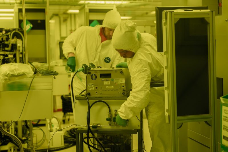
A dramatically updated Virginia Tech Micro/Nanofabrication Cleanroom and Laboratory ushers in a new era of semiconductor innovation.
And it’s all thanks to a $3 million gift-in-kind of semiconductor processing and manufacturing equipment in 2019 driven by SPTS Technologies’ CEO at that time, Kevin T. Crofton ’82.
“As an alum, I’ve always wanted to give back,” said Crofton, who is the namesake for Virginia Tech’s aerospace and ocean engineering department. “I feel like Virginia Tech has the opportunity to be not only the center of advanced research and development that's needed in the semiconductor industry, but also a center to cultivate talent and expand the university footprint. With a very modern clean room, Virginia Tech will have the opportunity to be on the leading edge of materials engineering and device process application to enable AI, high-performance computing, and emerging tech needs.”

After an extensive revitalization, the clean room is reopened and ready to serve as a space for advanced research and collaborations with groups such as the Virginia Alliance for Semiconductor Technology.
Established in 2006 as the Micron Technology Semiconductor Processing Laboratory, the clean room is a state-of-the-art facility supporting cross-disciplinary researchers and students in a collaborative environment for semiconductor manufacturing. Semiconductors are the building blocks for modern electronics and require highly controlled environments to minimize contaminants such as dust, particles, and even airborne microbes.
With the recent upgrades, the lab expanded into a second location: the Nanoscale Characterization-Fabrication Lab, which is supported and managed by the Institute for Critical Technology and Applied Sciences in the Virginia Tech Corporate Research Center. The clean room already boasted machines for etching, thermal treatment, and device packaging, new equipment to the lab includes the following:
- JEOL JBX 8100FS Electron Beam Lithography System, a cutting-edge instrument that creates delicate patterns on computer chips and other surfaces by using a precise beam of electrons. The system is located in the Corporate Research Center.
- Kurt J. Lesker plasma-enhanced atomic layer deposition system, a machine that utilizes special chemicals to create atomically controlled, thin layers of material.
- DELTA PECVD, a chemical vapor deposition tool that deposits high-quality insulation films such as silicon dioxide and silicon nitride.
- Two separate material etchers: the OMEGA ICP etcher and the Rapier DRIE. The former etches oxides, nitrides and other materials using very hot, electrically charged plasma, while the latter is engineered for high-rate silicon etching.
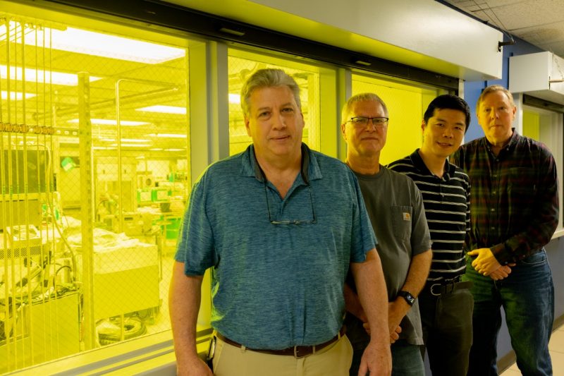
“The generous support from SPTS Technologies and Kevin Crofton in securing this state-of-the-art equipment serves as a powerful testament to the profound impact that alumni engagement can have on the university's trajectory,” said Wei Zhou, faculty director for the clean room and associate professor in the Bradley Department of Electrical and Computer Engineering. “This partnership exemplifies a shared commitment to pushing the boundaries of knowledge and nurturing the next generation of leaders. It will ignite a spark of inspiration in our students, demonstrating the transformative power of investing in one's community.”
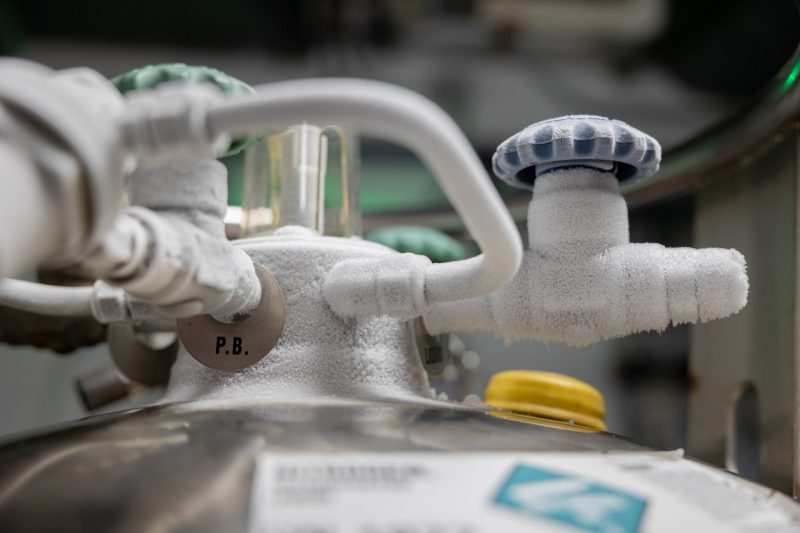
In addition to the equipment, the clean room located in Whittemore Hall has been modernized; the ventilation, gas delivery and water-cooling systems have been meticulously upgraded. These systems are essential to maintain stable temperatures, pristine air filtration, and ventilation needed for the delicate fabrication of semiconductors.
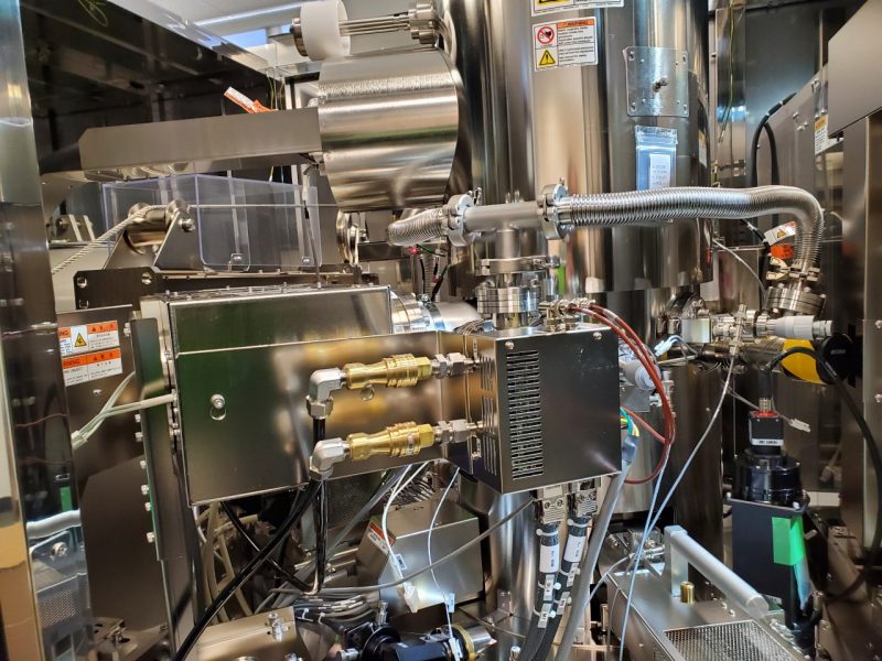
The electron beam lithography system will play a large role in that process. As one of the most advanced lithography instruments in the country, it empowers researchers to craft intricate nanostructures with unprecedented accuracy, unlocking the potential for transformative breakthroughs in
- Quantum computing: Technology that leverages the principles of quantum mechanics to perform calculations faster than traditional computers. Quantum computing has many future applications, including machine learning and cryptography.
- Nanophotonics: The study and manipulation of light at the nanoscale. Nanophotonics are used in sensors, solar cells, and lasers.
- Microelectronics: The design and fabrication of electronic circuits on a small scale. They're found in computers, smart phones, medical devices, cars, and industrial automation.
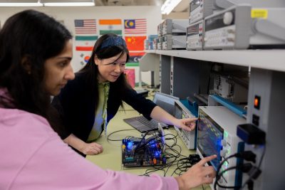
After years of work to update the clean room, Zhou is eager for students, faculty, and researchers to benefit from the cutting-edge equipment and facilities. Southwest Virginia high school students were already able to explore the clean room as part of the UPWARDS 2024 summer camp, which is designed to encourage young women in joining the semiconductor industry.
“The presence of such powerful tools on our campus represents a quantum leap in our research capabilities,” Zhou said. “The clean room fosters a collaborative ecosystem, and we aim to accelerate innovation, drive economic growth, and address critical challenges in society. The clean room will serve as a training ground for the next generation of innovators, equipping them with the skills and knowledge to make a real difference in the world.”
Related stories



.jpg.transform/s-medium/image.jpg)